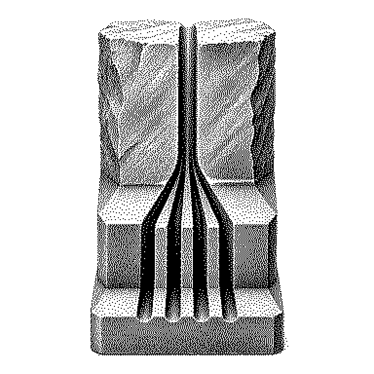
Self-Aligned Quadruple Patterning
Self-Aligned Quadruple Patterning (SAQP) is a trick from chip manufacturing that turns a single drawn line into four extremely fine lines. This makes it possible to create structures smaller than anything the exposure machine could actually image on its own.
Computer chips are made by transferring tiny patterns onto a slice of silicon. To do this, the wafer is exposed to light, somewhat like how a photograph used to be developed. Every exposure machine has a limit: beyond a certain fineness, the lines blur together. Self-Aligned Quadruple Patterning is a process that gets around this limit. Coarser lines are exposed first and then quadrupled through several chemical processing steps. In the end, four times as many lines sit on the wafer, each only a quarter as far from its neighbor as before.
Why chipmakers take this detour
Chips only become faster and more energy-efficient if the components on them move closer together. The exposure machines needed for this cost several hundred million euros apiece. Worldwide, there is only one manufacturer capable of building the most advanced models. Anyone without access to these machines needs a different route to fine structures.
This is exactly where SAQP comes in. With an older, weaker machine, very fine patterns can still be produced if one accepts more processing steps. It’s a trade-off: an expensive machine swapped for a more elaborate manufacturing process. For countries under export restrictions, this trade-off is often the only option.
The price for this is high. Every additional step takes time, consumes material, and can introduce errors. If a single step goes wrong, the entire chip becomes scrap. As a result, yield—the share of functioning chips per wafer—drops. Experts disagree on the point at which this stops being economically worthwhile.
From one line to four lines
At the core of the process are so-called spacers, meaning thin sidewalls. First, a relatively wide auxiliary line is exposed and shaped. A hairline-thin layer of material is then deposited over it, coating the line evenly. The top is then etched away. What remains are just two narrow walls, one on each side of the auxiliary line.
The auxiliary line itself is now removed. One line has thus become two walls, spaced twice as densely. This sequence is called double patterning. Repeating it with the two walls as new templates produces four lines. Hence the name quadruple, meaning fourfold.
The qualifier “self-aligned” is crucial. The new lines are not realigned; they inevitably form directly at the edges of the old ones. The physics of the coating process determines the spacing, not a machine repositioning a mask. This eliminates a major source of error: the imprecise overlay of two exposures. The downside is that this mainly succeeds in producing regular stripe patterns. Irregular shapes have to be cut out afterward in further steps.
SAQP in news coverage of chip manufacturing
The term usually shows up in reports about the dispute over semiconductor technology. When a Chinese manufacturer announces a chip in a very fine process class, the question of the method used often follows. The answer is frequently: multiple patterning using older exposure machines. Analysts then estimate just how expensive and error-prone these chips are likely to be.
SAQP is also widespread in memory chips. There, millions of identical cells sit in strict rows, and regular patterns are exactly where this process excels. It’s therefore very likely that smartphones and graphics cards contain technology built using spacers.
A common misconception is that SAQP is a substitute for modern exposure technology. It is more of a crutch with clear limits. For processors with irregular circuitry, the number of steps eventually becomes unaffordable. So the term is less a promise than an indication of the constraints under which a chip was built.