Overlay Error
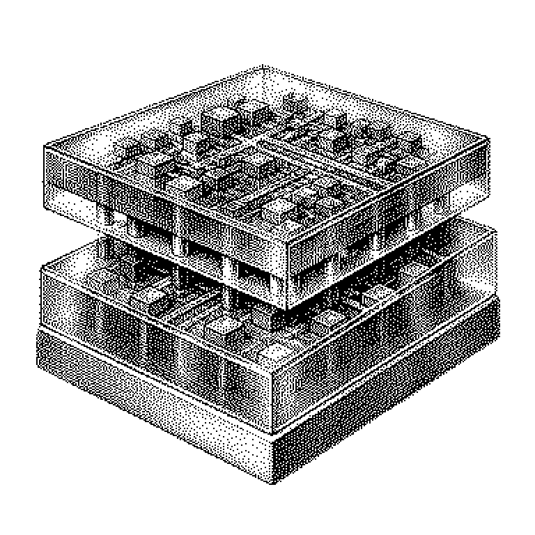
An overlay error is a tiny misalignment between two layers that are placed on top of each other during the manufacturing of computer chips. If the layers don't line up exactly, the circuits built into them no longer function reliably.
Computer chips are not manufactured in one piece, but built up layer by layer. On a thin silicon wafer, dozens of layers of metal and insulating material are formed one after another. Each new layer must sit precisely over the one beneath it, because the layers are connected by fine vertical links. Overlay error describes how far one layer is shifted, rotated, or distorted relative to the previous one. It is measured in nanometers, i.e. in millionths of a millimeter. A comparison helps: it’s like printing a color image where cyan, magenta, yellow, and black are applied to the paper one at a time — if one color is slightly off, the image looks blurred.
Why a few nanometers decide millions of euros
In modern chips, individual components are only a few nanometers in size. The vertical connections between the layers are similarly small. If a layer shifts too much, a connection no longer fully reaches its target. Electrical resistance increases, and in the worst case the connection breaks off entirely. The chip is then scrap.
The problem lies in the sheer volume. A silicon wafer holds hundreds of chips, and a single factory processes tens of thousands of wafers per month. A systematic overlay error doesn’t affect just one chip, but entire batches. That’s why so-called yield — the share of functioning chips — is one of the industry’s most important metrics. Just a few percentage points of difference can shift a plant’s profit significantly.
This matters to investors because chip companies often address their yield indirectly in quarterly reports. Phrases like “ramp-up challenges with the new manufacturing generation” usually mean precisely these kinds of precision problems. Overlay is one of the major cost drivers here, because it becomes harder to control with every new chip generation.
Alignment marks, feedback loops, and the limits of the machine
The layers are created through exposure. A machine, the exposure tool (or stepper), projects the pattern of a mask onto the wafer. So that the machine knows where the previous layer lies, tiny alignment marks were printed there along with it. A measuring device scans these marks and calculates the deviation. The exposure tool then shifts the wafer or the optics before exposing the next layer.
This feedback loop runs continuously. The software breaks the measured deviation down into components: a uniform shift of the entire wafer, a slight rotation, a stretch. Uniform components can be calculated out fairly easily. What remains is an irregular residual error, and this residual is the difficult part.
Causes include, for example, heat that minimally expands the wafer, mechanical stresses in the applied layers, or minimal deformations of the mask. This is increasingly where machine learning comes in: models analyze measurement data from many wafers and predict the deviation of the next wafer. The correction is then applied before the error even occurs. It’s important to distinguish this from resolution: resolution describes how small a structure a machine can image at all. Overlay describes how precisely it places those structures. Both have to be right.
Overlay in quarterly figures and factory reports
In everyday life, one rarely encounters the term directly, but its consequences are common. When a smartphone processor launches later than planned or a graphics card stays in short supply, manufacturing problems are often behind it. Overlay is one of the reasons why new chip generations take months before they run at high volume.
In business news, the term comes up in the context of machine builders and chip fabs. Manufacturers of exposure systems advertise overlay values in the range of just a few nanometers, because that’s their key selling point. Providers of metrology equipment and analysis software also profit directly from this problem.
A common misconception is that overlay errors are the result of sloppiness or carelessness. That’s false. They are an unavoidable physical limit, and manufacturing means keeping that limit within a narrow tolerance window. Anyone who wants to understand chip industry news should therefore think of overlay as an ongoing issue, not a one-off incident.