Quadruple Patterning
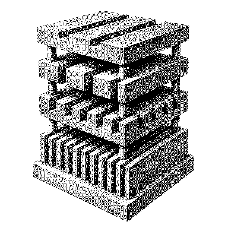
Quadruple patterning is a trick from chip manufacturing: instead of exposing a very fine structure directly, it is created in four steps from coarser structures. This makes it possible to fabricate circuit traces finer than the exposure machine can actually draw.
Computer chips are made by projecting tiny patterns onto a silicon wafer using light. This process is called lithography, and it has a hard limit: very fine lines can no longer be cleanly imaged with light of a given wavelength. Quadruple patterning is a way around this. Instead of exposing one extremely fine pattern, four coarser patterns are cleverly layered on top of each other. In the end, the wafer bears a grid of lines that is four times as dense as what a single exposure can achieve. For years, this technique was a key building block for building ever smaller chips.
The price of smaller chips
Chips have been getting more powerful for decades because their components keep shrinking. Smaller transistors mean more computing power per area and lower power consumption. When the available light from exposure machines became too coarse, this progress threatened to stall. Quadruple patterning delayed that standstill by several chip generations.
The price for this is high. Each additional step costs time, material, and machine hours in a factory worth many billions of euros. A chip that needs four exposure passes per layer is significantly more expensive than one that needs only one. The error rate also rises: at every step, something can slip slightly out of alignment.
This is exactly why the shift to EUV lithography was such a big topic in the industry. EUV stands for extreme ultraviolet light, which has a much shorter wavelength and can directly expose finer structures. Wherever EUV is used, a single step often replaces the four steps of quadruple patterning. The Dutch manufacturer ASML is the world’s only supplier of these machines, which makes it one of the most important companies in the chip industry.
Four steps to a fine grid
The most common variant is called self-aligned quadruple patterning. The basic idea can be explained using a stencil. First, relatively wide strips are drawn onto the wafer. Then a thin layer is deposited on the vertical edges of these strips. The original strips are then etched away. What remains are only the thin sidewalls, and each strip has become two fine lines.
This trick is repeated a second time. The two lines become four, so the density has quadrupled overall. Crucially, the width of the sidewalls does not depend on the light but on the thickness of the deposited layer. That thickness can be controlled very precisely, down to the range of just a few atomic layers.
A common misconception is that this process could be repeated indefinitely. In practice, that’s not possible. With each pass, tiny inaccuracies accumulate, and the lines become unevenly wide. Moreover, this technique is mainly suited to creating regular grids, not arbitrarily branching shapes. Interruptions and branches must be cut in using additional steps.
Where the technique shows up in chip news
In everyday life, you encounter quadruple patterning in every smartphone and every graphics card, without anyone mentioning it. It is used in the manufacturing of modern processors and especially in memory chips, whose structure consists of regular grids. Flash memory and RAM benefit greatly from the technique.
In business news, the term usually comes up in connection with manufacturing costs. When manufacturers like TSMC, Samsung, or Intel talk about new process nodes, the discussion often centers on how many exposure steps are required. Fewer steps mean higher yield and better margins.
The topic also plays a role in the debate over export controls. Chinese manufacturers do not have access to EUV machines. They therefore try to manufacture modern chips using older technology and multiple patterning. This works technically, but it is more expensive and yields fewer usable chips per wafer. Quadruple patterning is thus not just a manufacturing detail, but also a point of contention in geopolitical discussions.