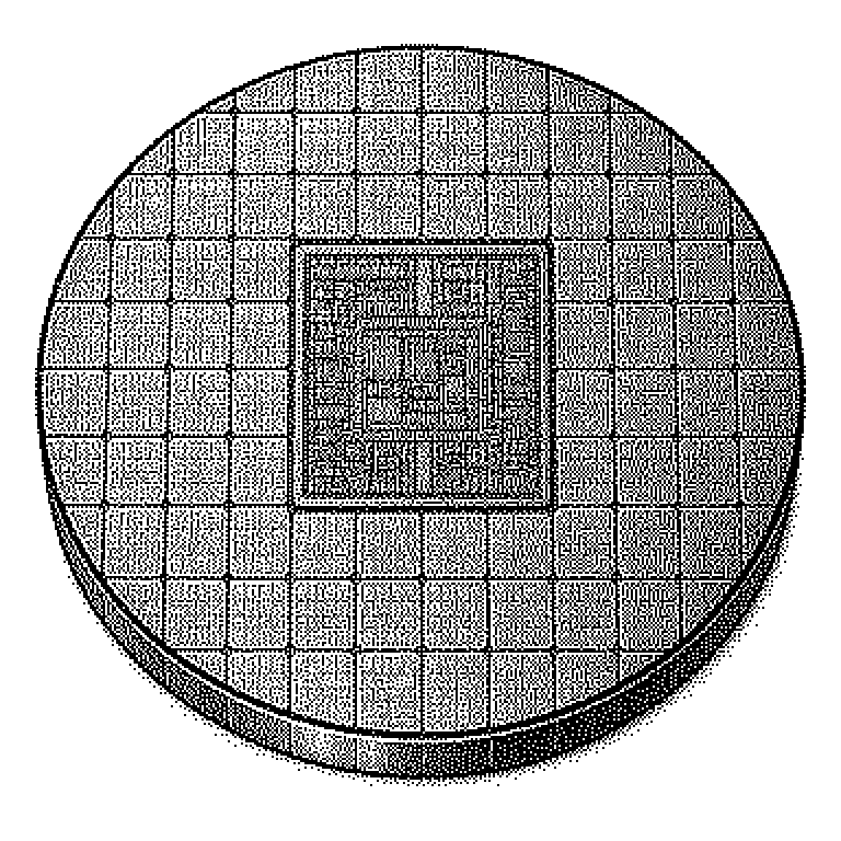
Die Size
Die size refers to the area of a single computer chip on the round silicon disc from which it is cut. It is given in square millimeters and largely determines how expensive a chip is to manufacture.
Computer chips are not made individually, but by the hundreds at once on a round disc of silicon. This disc is called a wafer and usually has a diameter of 30 centimeters. At the end of production it is sawn apart, and each cut-out rectangle is a finished chip. This single rectangle is called a die in technical jargon, pronounced like the English word “dai”. The die size is simply the area of such a rectangle, given in square millimeters. Small chips for smartphones are around 100 mm², while large graphics and AI chips reach over 800 mm².
Why square millimeters decide billions
A wafer costs a fixed amount to manufacture, regardless of what is produced on it. With state-of-the-art fabrication, that is several tens of thousands of dollars per disc. The price per chip therefore results almost directly from how many chips fit on the disc. If you halve the die size, the yield roughly doubles and the unit price drops accordingly.
There is a second effect that is often underestimated. Every wafer develops randomly distributed defects, tiny flaws in the material or in the exposure process. A defect usually renders the entire chip it sits in unusable. With small chips, a defect only affects a small piece of area. With a very large chip, the probability is high that a defect will land somewhere on it.
That is why costs rise with area not linearly, but disproportionately. A chip with twice the area costs significantly more than twice as much. This is exactly why large AI accelerators carry five-figure prices, while a phone chip falls in the low double-digit range.
What engineers do about chips that are too large
The area is determined by the number of transistors, the tiny switches that make up a chip. More computing power requires more transistors, and more transistors require space. The classic way out is finer manufacturing: with each new generation, the structures become smaller, so more transistors fit into the same area. Labels like “3-nanometer process” refer to this miniaturization, even though the number today is more of a marketing name than an actual measurement.
This shrinking runs into physical limits and keeps becoming more expensive. That is why the industry increasingly relies on a second strategy, so-called chiplet design. Instead of one huge die, several smaller ones are built and connected within a shared package. Each individual piece then achieves better yield, because a defect only ruins one part.
There is, however, a hard upper limit. The lithography machines can only image a field of about 26 by 33 millimeters per exposure, around 858 mm². This limit is called the reticle limit. Anyone wanting to build larger must inevitably assemble multiple dies.
Die size in product announcements and quarterly earnings
In reviews of processors and graphics cards, the die size is usually listed right next to the transistor count. It allows for a fair comparison between manufacturers: whoever delivers the same performance in less area is working more efficiently. Experts often calculate transistor density for this purpose, meaning millions of transistors per square millimeter.
The topic also comes up in financial news, though rarely under this name. When a manufacturer complains about declining margins, an oversized and therefore expensive chip is often behind it. Conversely, a compact design is considered a competitive advantage, because the same scarce manufacturing capacity yields more sellable product.
A common misconception is that a larger chip is automatically the better one. Area alone says nothing about performance, only about material consumption. What matters is always the ratio of performance to area and power consumption.