Chiplet
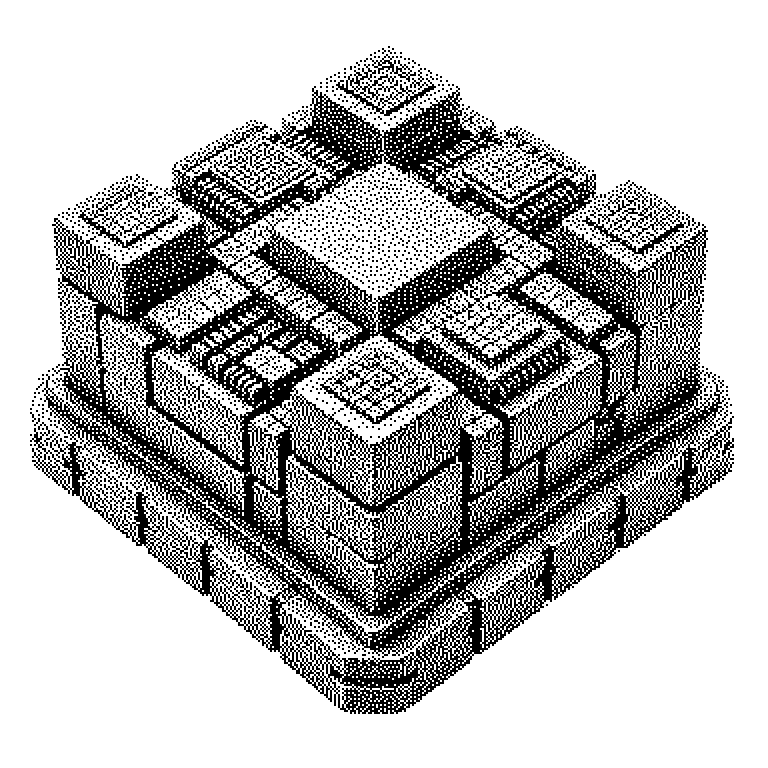
A chiplet is a small silicon building block that is assembled together with other such building blocks in a shared package to form a large processor. This construction method is cheaper and more flexible than manufacturing an entire processor from a single piece.
A processor is the computing part in computers, phones, and servers. For a long time it was manufactured as a single large piece of silicon, that is, from one continuous slab. Today manufacturers often assemble it from several small pieces. These small pieces are called chiplets. They sit side by side or stacked in a shared package and are connected to each other via fine traces. From the outside, the whole thing behaves like a single processor.
Why large chips made in one piece are so expensive
Silicon is manufactured in round discs called wafers. Many chips are produced simultaneously on such a disc. In the process, tiny defects inevitably occur, scattered across the entire disc. Every chip affected by such a defect becomes scrap.
This is where the decisive computational advantage of chiplets lies. If a chip is very large, a defect is likely to hit it, and an expensive component ends up in the trash. If the chips are small, the same defect only affects a small piece. The rest of the disc remains usable. The proportion of functioning chips, called yield in the industry, increases significantly as a result.
Added to this is flexibility. A manufacturer can use the same compute chiplet in an inexpensive laptop processor and in an expensive server chip, simply in different quantities. This means they don’t have to develop a completely new design for every product variant. That saves development time and a lot of money.
How the individual parts come together
You can imagine a chiplet processor like an apartment made of prefabricated modules. Kitchen, bathroom, and living space are produced separately and only connected on the construction site. In processors, a carrier plate in the package takes on the role of this construction site. It is called an interposer or substrate and contains the connections between the chiplets.
The connections must be extremely fast. Data flows between two chiplets at a magnitude at which normal circuit board traces would be hopelessly too slow. That’s why the chiplets lie very close together, and are sometimes even stacked on top of each other. For the language in which they communicate with one another, there is now an open industry standard called UCIe.
Another advantage: not every chiplet has to be built using the same manufacturing process. The compute cores are made using the most expensive and most modern process. Connections for USB or memory, on the other hand, also work fine with older, much cheaper technology. This exact mixture is one of the main reasons why this construction method has become established.
Chiplets in current processors and AI accelerators
AMD brought this construction method into widespread use in its Ryzen and Epyc processors starting in 2019, gaining a lot of ground on Intel in the process. Intel has since also switched to chiplets, usually calling them tiles there. Apple also uses the principle: the M Ultra chip consists of two connected individual chips.
Chiplets are especially important in graphics and AI accelerators. Nvidia's and AMD's compute cards for data centers consist of several silicon building blocks plus stacked memory blocks in the same package. Without this construction method, such chips would simply be too large to manufacture. When business news talks about bottlenecks in so-called advanced packaging, it is referring precisely to the assembly of these building blocks.
A common misconception is that chiplets are the same as multiple compute cores. That’s not correct. Cores have existed within a single chip for a long time. Chiplets don’t describe the computing structure, but rather the physical construction method: several separately manufactured pieces of silicon in one package.