Wafer-Scale Chip
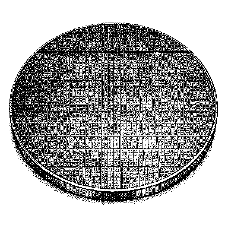
A wafer-scale chip is a single computer chip that is as large as the round silicon disc from which hundreds of small chips are normally cut. Such chips are built primarily to perform very large AI computations without slow connections between individual components.
Computer chips are made from thin, round discs of silicon called wafers. Such a wafer often has a diameter of around 30 centimeters. Normally, hundreds of small chips are manufactured on it simultaneously and then cut apart. A wafer-scale chip breaks with this rule: it is not cut up, but remains a single giant component. Instead of an area the size of a fingernail, you get a chip the size of a small plate. The best-known example comes from the company Cerebras, whose chip combines several hundred thousand compute cores on a single disc.
Why proximity on the chip brings so much speed
Large AI models are trained today on thousands of graphics cards simultaneously. These cards must constantly exchange intermediate results. The path via cables and connectors is the bottleneck here. Data within a chip flows many times faster than data between two chips.
A wafer-scale chip moves many of these paths inward. What used to be a cable between two cards is now a short trace on the same disc. This saves time and power, since every signal that leaves the chip costs comparatively a lot of energy. For tasks in which very many compute cores must work closely together, this is a real advantage.
There is also a practical point: a single device is easier to program than a network of many. Anyone distributing a model across a thousand graphics cards has to split up the work by hand. On a very large chip, part of this splitting can be eliminated. This shortens development time, even though it never makes things entirely simple.
Dealing with defects in the silicon
During chip manufacturing, tiny defects always occur in the material. For normal chips, this is manageable. You throw away the few broken specimens and sell the good ones. For a chip that occupies the entire wafer, this calculation no longer works. A single defect would render the entire component unusable.
The solution is called redundancy: more compute cores are deliberately built in than are needed. After production, it is checked which areas are defective. These are permanently switched off and replaced by reserve cores. The chip then continues to work quite normally, just with a slightly different internal layout.
Two further problems are heat and power. A chip of this size can draw over ten kilowatts, as much as several electric heaters. That is why it sits in its own housing with water cooling and an elaborate power supply from above rather than from the side. This should not be confused with the so-called chiplet approach: there, several small chips are packed tightly next to each other, but remain separate components.
Who actually uses such chips
A wafer-scale chip will never sit in your own computer or phone. It is a specialized device for data centers and costs several million euros depending on the system. Buyers are research labs, government supercomputing centers, and companies that want to train their own AI models. Applications from weather forecasting and drug research also run on such hardware.
In business news, the term usually appears in connection with the competition for AI computing power. The market has so far been clearly dominated by Nvidia and its graphics cards. Companies like Cerebras are trying to counter this with a completely different design principle. Whether this prevails depends less on the technology than on the software, since mature programming tools have existed for Nvidia cards for years.
A common misconception is that a bigger chip is automatically the faster one. This only holds true for certain tasks. If a computation can be cleanly broken down into independent parts, many ordinary chips are often cheaper and more flexible. The wafer-scale approach only shows its strength where data exchange is the actual bottleneck.