Wafer-Scale Chip
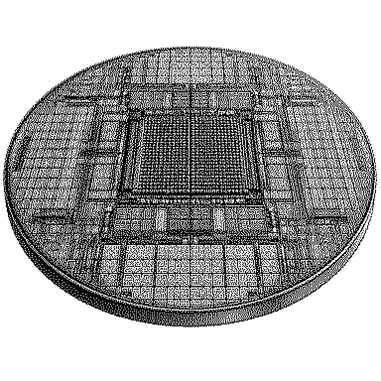
A wafer-scale chip is a single computer chip that is as large as the round silicon disc from which hundreds of small chips are otherwise cut. It is mainly built for training AI models because it combines a huge number of compute units without slow connections between components.
Computer chips are made from round silicon discs known as wafers. These discs are typically 30 centimeters in diameter. Normally, hundreds of small chips are cut out of a single wafer and individually packaged into casings. A wafer-scale chip breaks with this approach: here, the entire disc remains a single, unified component. The result is a computing surface of around 46,000 square millimeters, roughly the size of a breakfast plate. By comparison, a typical AI graphics processor is barely larger than a postage stamp.
Why a plate computes better than 60 postage stamps
Large AI models have long since outgrown a single processor. That’s why they are distributed across many chips, which must communicate with each other via cables and networking technology. This communication is precisely the bottleneck. Sending data from one chip to the next takes many times longer than movement within the same chip. A significant portion of expensive computing time is spent waiting.
A wafer-scale chip moves these pathways inward. What was previously a network cable is now a copper trace within the silicon. The signals travel shorter distances, consume less energy in the process, and arrive faster. For tasks that involve constantly exchanging intermediate results, this brings measurable advantages.
There’s also a practical point: building a computing cluster out of hundreds of individual accelerators is complex. You need racks, cabling, cooling, and software that distributes the workload properly. A single large component replaces part of this complexity. This is an argument that providers like Cerebras regularly make to customers.
Dealing with defects in the silicon
Defects inevitably occur during chip manufacturing. A speck of dust or an inaccuracy in the lithography process renders a small area of the wafer unusable. In normal production, this is manageable: the affected chips are discarded, and the rest are sold. With a wafer-scale chip, this way out doesn’t exist. A single defect would theoretically destroy the entire product.
The solution is called redundancy. The chip is built from tens of thousands of identical compute cores arranged in a grid. After manufacturing, the cores are tested to see which ones work. The defective ones are permanently disabled and replaced by spare cores that are planned in from the start. The connections in the grid are rerouted so that the gap goes unnoticed. As a result, the chip loses a bit of performance but remains functional.
A second problem is physics. Such a component draws several kilowatts of power, roughly as much as an electric kettle, and requires elaborate cooling. Furthermore, silicon expands differently under heat than the circuit board beneath it. At postage-stamp size this doesn’t matter, but at plate size, the contacts would otherwise crack. Manufacturers therefore need specially developed mounts and water cooling.
A niche in the shadow of GPU data centers
In the news, the term usually appears in connection with the company Cerebras, which has been pursuing this approach since 2019. Their products are called Wafer Scale Engine and are sold to research institutions, pharmaceutical companies, and data center operators. Cerebras’s IPO was also a topic in the business press. Other providers, such as Tesla with its Dojo project, have tried similar approaches.
In everyday life, one only encounters this technology indirectly. Anyone using a chat service that responds especially fast may, under certain circumstances, be computing on such hardware. As a private individual, you cannot buy a wafer-scale chip, if only because a single system costs several million euros.
A common misconception is that these chips will replace conventional graphics processors. So far, that doesn’t seem to be the case. The market is clearly dominated by Nvidia, and the majority of AI software is tailored to its systems. Wafer-scale chips are more of a specialized answer to a specialized problem: very large models, very tight coupling, very little tolerance for latency.