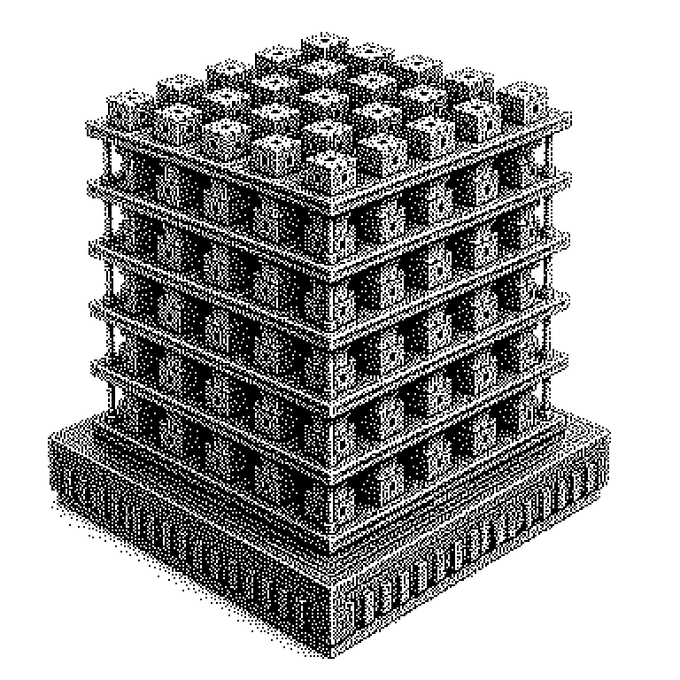
3D NAND
3D NAND is a construction method for memory chips in which the memory cells are stacked in many layers on top of each other instead of merely side by side. This allows significantly more data to fit on chips of the same size – the technology is now found in almost every SSD, in smartphones, and in memory cards.
Inside smartphones, digital cameras, and modern laptops sits a type of memory that retains data even without power. It consists of tiny cells, each of which can hold a small amount of electrical charge. Whether a cell is charged or not corresponds to a zero or a one. In the past, these cells all lay next to each other in a single layer, like houses in a flat housing development. With 3D NAND, however, they are built in many layers stacked on top of one another, like apartments in a high-rise. This allows a multiple of the data to fit in the same area.
Why flat memory chips hit their limit
For decades, memory chips became cheaper simply by shrinking the cells. The smaller a cell, the more of them fit on a slice of silicon. But at some point the cells became so small that only a few dozen electrons carried the stored information. Such cells lose their charge more easily and interfered with their direct neighbors. The chips were no longer getting better, but rather more unreliable.
The way out was to go upward. A single cell is allowed to be somewhat larger and more robust again if many layers are stacked instead. The first chips of this kind had around 24 to 32 layers. Today, over 200 layers are standard, and manufacturers are working on more than 400. This is precisely the reason why a one-terabyte SSD today costs a few dozen euros instead of several hundred.
This is directly relevant for the AI industry. Training data for large models consists of enormous collections of text and images that must be read quickly. Conventional hard drives with rotating platters deliver the data too slowly for this. Without cheap flash memory, building today’s data centers would hardly be economically feasible.
Holes through the stack: how the layers are built
A 3D NAND chip is not created by gluing finished chips on top of each other. Instead, layers of conducting and insulating material grow alternately on a silicon wafer. Only once this stack is complete does a machine etch vertical holes through it – sometimes several micrometers deep with a diameter of less than a ten-thousandth of a millimeter. The material that will later store the charge is deposited into these holes. Every intersection of a hole and a conducting layer is a memory cell.
The great advantage: a single etching step simultaneously creates all the cells of a tower. More layers therefore cost hardly any additional process steps. The difficulty lies in the fact that the hole must be equally wide at the top and at the bottom. If it narrows toward the bottom, the lower cells behave differently than the upper ones.
In addition, modern cells store not just one bit but three or four. To do this, the control electronics distinguish between several charge levels instead of just “full” and “empty.” This further increases capacity but makes the cells more sensitive and limits their lifespan. A cell can only be rewritten a limited number of times, often in the range of a few hundred to a few thousand cycles.
3D NAND in devices and in quarterly results
Practically every memory you can buy that retains data without power is now 3D NAND. This applies to SSDs in laptops, the internal storage of phones, USB sticks, and camera memory cards. It is important to distinguish this from working memory, called DRAM: it is faster, but forgets everything as soon as the power is gone.
In business news, the term mainly comes up in connection with the manufacturers. Samsung, SK Hynix, Micron, Kioxia, and Western Digital practically divide the market among themselves. Their revenues fluctuate strongly because memory is an interchangeable commodity. If there are too many chips, prices crash; if supply is tight, manufacturers earn billions in a single quarter. Reports like “Micron starts mass production with over 200 layers” are therefore not purely technical news, but a signal about future prices.