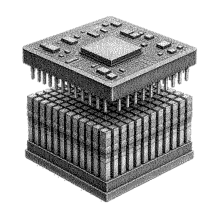
Xtacking
Xtacking is a manufacturing process from the Chinese memory maker YMTC in which the control electronics of a memory chip are fabricated separately and then placed on top of the actual memory cells. This makes chips faster and denser, without both parts having to make the same manufacturing compromise.
Almost every smartphone and every SSD contains memory chips that retain data even without power. Such a chip consists of two very different parts. One part is billions of tiny memory cells that hold the data. The other part is the control electronics, which decide which cell is currently being read or written. Normally, both parts are fabricated side by side on the same silicon wafer. Xtacking is a process from the Chinese manufacturer YMTC in which they are manufactured separately and then placed on top of one another. The name alludes to the English word “stacking”.
Why separate manufacturing yields more storage per chip
Memory cells and control electronics have opposing requirements. Cells should be as dense and as cheap as possible. The control electronics, on the other hand, should switch as fast as possible, which requires more modern transistors. If both are manufactured together, a compromise must be made. Both parts then get a process that is not ideal for either of them.
Separate manufacturing resolves this conflict. The cells are created on one wafer using a process optimized for density. The control electronics are created in parallel on a second wafer using a faster process. Afterward, the two are joined. Each part therefore gets exactly what it needs.
The second benefit is area. If the control electronics sit below or above the cells instead of next to them, the space beside them becomes free. This allows more memory cells to fit on the same chip area. YMTC cited area gains of around a quarter for early Xtacking generations. For customers, this means more gigabytes per chip at the same price.
Billions of contacts between two silicon wafers
The decisive step is joining the two wafers. On the top surface of each wafer sit tiny metal pads, the contact points. The wafers are aligned with extreme precision and then pressed together. Upon contact, the metal pads bond permanently. This is referred to as wafer bonding, where a wafer is a thin silicon disc.
This connection consists of billions of individual contacts at once. They are short and lie directly on top of one another. Short paths mean less delay, which is why the chip can deliver data to the outside faster. This is exactly what Xtacking aims for: higher transfer rates per memory chip.
The price for this is precision. The alignment must be accurate to within a few nanometers, a nanometer being one millionth of a millimeter. If one wafer is slightly misaligned, the entire assembly becomes unusable. In that case, two good wafers are lost instead of one. That is why the process is technically demanding and only pays off at large production volumes.
Where Xtacking shows up in devices and headlines
Xtacking is used in NAND flash, the type of memory used by SSDs, USB sticks, and smartphones. Anyone who buys an SSD from YMTC or its consumer brand Zhitai has this process inside their device. Some smartphone manufacturers have also used YMTC memory. The term rarely appears on packaging, but it does show up in datasheets and reviews.
In the news, the term usually comes up in connection with the dispute over chip technology between the US and China. YMTC has been on US trade lists since 2022 and has more difficulty accessing Western manufacturing equipment. Xtacking is seen as an example that a manufacturer can build competitive chips even with older machines if the architecture is clever. For this reason, the process is often cited as a symbol in analyses.
A common misconception is confusing it with 3D NAND. In 3D NAND, the memory cells themselves are stacked in many layers, today well over 200. All major manufacturers do this. Xtacking, by contrast, additionally stacks the control electronics on top of this cell block. Both ideas therefore complement each other; they do not replace one another.